Reasons for HDI-Printed Circuit Boards

Why Choose HuaXing as Your HDI PCB Supplier?
Cost reduction via HDI-printed circuit boards
Fewer layers Reduced circuit board size Miniaturization enhances competitiveness
HDI-printed boards empower high technology
Increased packing density Facilitates placement of BGAs with minimal pitch Streamlines placement for CSP (Chip Scale Package) or Flip Chip
Enhanced capabilities of HDI-printed boards.
Enhanced power stability Reduced interference from inductance and capacitance Improved signal integrity for high-speed designs

Benefits of HDI PCBs

Cost efficiency

With strategic planning, HDI technology can cut overall costs compared to standard PCBs, thanks to fewer layers, smaller dimensions, and reduced PCB quantities required.

Improved signal integrity

HDI technology employs via-in-pad and blind-via techniques to bring components closer, shortening signal paths and improving signal integrity.

Enhanced reliability

Microvias offer superior reliability to through-hole vias due to their smaller aspect ratio and better materials, enhancing HDI technology performance.

Various Via Types in HDI PCBs

01

Through hole via

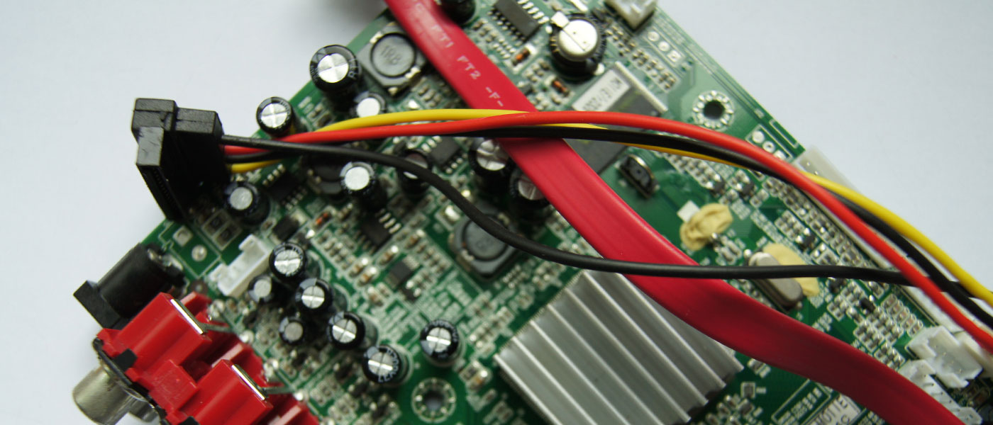
Through hole via is openings that extend from one side of the circuit board to the other, allowing components like pins, sockets, or other parts to be soldered through them.

02

Blind via

A blind via is a hole that connects an outer layer to an inner layer but doesn't traverse the entire PCB. These holes can be created either mechanically or through laser technology.

03

Burid via

This is a hole that passes through one or more inner layers, usually created through mechanical drilling.

04

Microvia

A Microvia is a blind structure with an aspect ratio of up to 1:1 between the diameter and depth of the hole, with a maximum depth of 0.25 mm measured from the surface to the target pad or plane.

HDI PCB Design Tips

FAQ: Your Guide to HDI PCB

Here are answers to some common questions and key considerations when choosing HDI PCB.

What is High Density Interconnector or HDI PCB?

What is High Density Interconnector or HDI PCB?

HDI PCBs, or High Density Interconnect boards, boast a higher wiring density than traditional PCBs.

What do you know about HDI Board ?

What do you know about HDI Board ?

HDI board stands for High-Density Interconnect, a relatively new technology in the PCB industry.

Who is the best HDI PCB manufacturer in China?

Who is the best HDI PCB manufacturer in China?

Huaxing, based in Shenzhen, specializes in producing and supplying china HDI PCBs. They offer competitive pricing and rapid turnaround times for both prototypes and mass production.

What is HDI-Printed Circuit Boards

What is HDI-Printed Circuit Boards

HDI printed circuit boards (High Density Interconnect) boast ultra-fine trace structures, tiny holes, and integrate Blind & Buried Vias (Microvias).

How to Determine if Your Product is pcb HDI?

How to Determine if Your Product is pcb HDI?

using microvias as connectors. These microvias serve as a way of directly connecting layers of leads and pads, which will allow a higher density of the board. That way, they enable the manufacturers to hide the wiring to the next layer.

How to reduce HDI PCB cost?

How to reduce HDI PCB cost?

Various factors can impact the cost of HDI PCB circuit boards. Understanding and selecting appropriate alternatives can result in savings on PCB manufacturing costs.

Let's Build Your Product