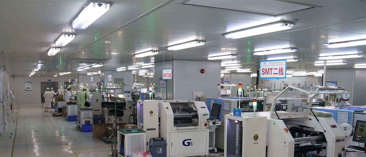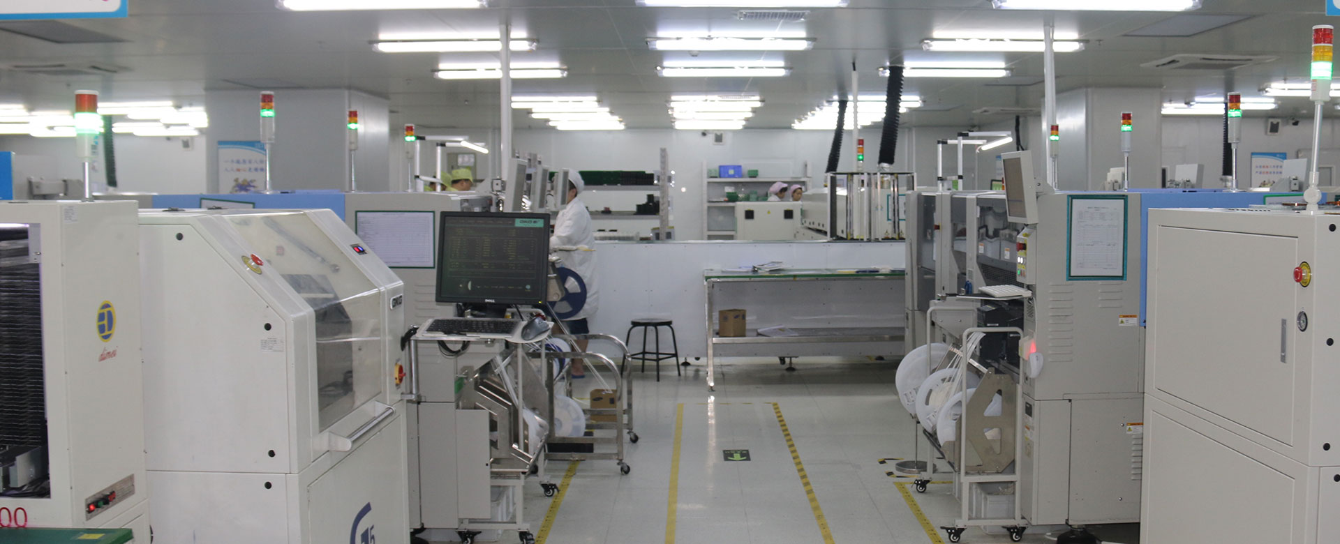
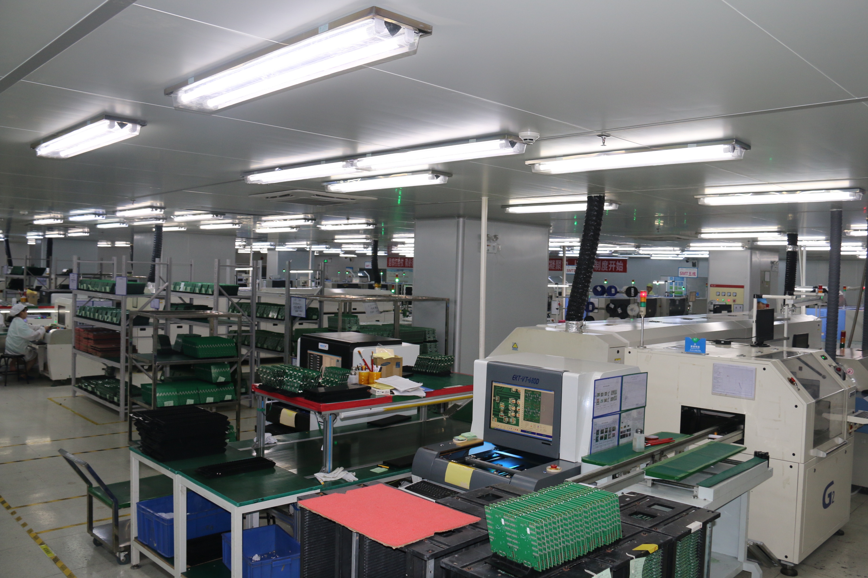
Surface Mount Technology (SMT) involves the direct mounting of electrical components onto a PCB's surface. This intricate process commences with the application of solder paste through stenciling, followed by the precise placement of parts onto the board pick-and-place machines. Subsequently, the PCB assemblies undergo reflow soldering in an oven to fuse the solder. Throughout the SMT process, various inspection points are integrated to uphold the utmost quality standards at each manufacturing phase.
This inspection method relies solely on experience, demanding a relatively high level of expertise from technicians. Unlike other testing methods, it does not necessitate the development of a test program; instead, it relies on intuitive visual inspection of the targeted area.
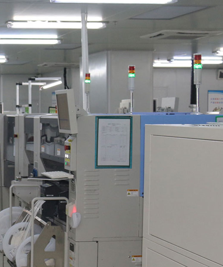
AOI utilizes a cutting-edge vision system, innovative lighting techniques, high magnification, and intricate processing methods to achieve a high defect capture rate swiftly from the surface. Primarily employed on production lines, this testing method focuses on detecting various defects during the operational process.
X-ray technology relies on a transmitter within the machine to emit high-energy electrons, generating X-rays for imaging samples by penetrating them. As X-rays interact differently with objects of varying densities, they produce distinct images, which subsequently reveal the location and morphology of defects within the sample.
Allow the use of smaller components.
Provide the maximum flexibility in constructing PCBs.
Reduce manual intervention in component placement.
Lower material costs.
Simplify the manufacturing process.