The utilization of multilayer circuit boards mitigates instability problems such as noise generation. This is achieved by enhancing interconnections and optimizing layouts, effectively addressing interference between components.
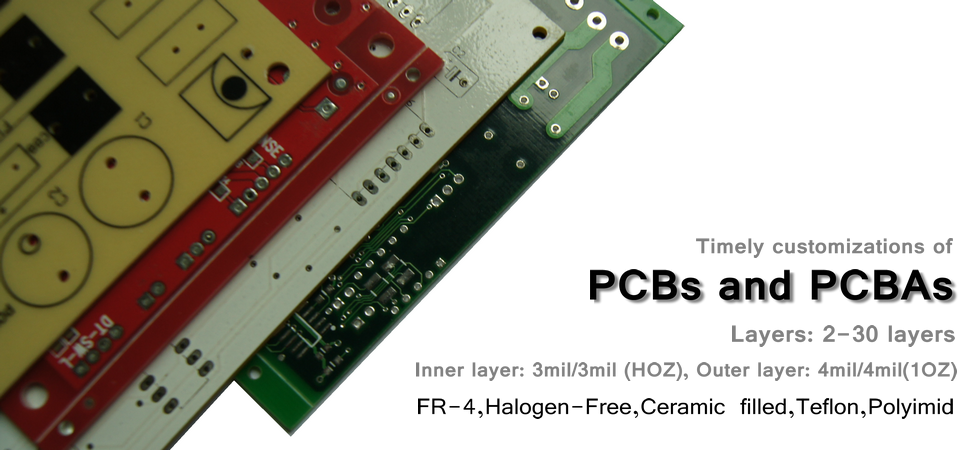
Multilayer PCBs stand out as ideal choices for contemporary communication equipment and intricate circuits, providing increased density and compact dimensions compared to single or double-layer alternatives.
In multilayer PCBs, the copper thickness within the holes surpasses that of standard single and double circuit boards, guaranteeing superior reliability.
Copper traces on a PCB facilitate the flow of current, but their inherent resistance can sometimes impede or alter the current, thereby affecting overall board performance. To mitigate this, controlled impedance traces are necessary to maintain signal integrity and power integrity.
To withstand potentially elevated temperatures, it is advisable to increase the thickness of copper traces beyond normal values. This adjustment helps regulate temperature, with the width of the traces being adjusted accordingly.
When current flows through individual components, it generates a magnetic field. In multilayer PCBs, the return path or ground plane serves as a shield, effectively managing these magnetic fields and providing a pathway for unwanted signals. To minimize electromagnetic induction issues, it's best to avoid using 90-degree traces.
Analysis of Requirements: Precisely outline functional and performance requirements.
Designing the Circuit: Develop circuit schematics and PCB layouts.
Signal Enhancement: Fine-tune layout to improve signal quality.
Planning Hierarchy: Strategize hierarchy and connections.
Component Packaging: Choose suitable packaging for components.
Evaluation and Validation: Scrutinize and validate the design.
Production and Assembly: Transfer the design to the manufacturing facility for production and assembly.