Choose The Right Option for Your Product

Your one-stop PCB source: explore our multilayer,

HDI, specialized options, and more.

Multilayer PCB
Designed for complex circuits requiring high functionality in compact spaces, ensuring reliability and superior signal integrity.
Rigid Flex Board
Combine flexibility with structural integrity, perfect for dynamic environments, offering streamlined packaging and enhanced connection reliability.
Aluminium PCB
Choose our Aluminium PCBs for high-power applications. Known for excellent heat dissipation, they ensure longevity and stability in LED lighting and power circuits.
Flexible PCB
Tailored for applications demanding durability and adaptability, offering exceptional conformability and resistance to vibrations and heat.
HDI PCB
Opt for our HDI PCBs when precision is key. With fine features and high-density components, they are ideal for advanced electronics requiring miniaturization without compromising performance.

We Turn Complex Components

into Elegant Products

Elevate your vision with our engineering and manufacturing expertise.
01. PCB Design and file
Upload your manufacturing data, typically in the form of Gerber files, which are standard for PCB production, detailing every aspect of the board's design.
2. Board Preparation
The base material, usually a type of fiberglass like FR4, is prepared by cutting it to the required size. This material forms the substrate of the PCB. Copper is then laminated onto this substrate to create a conductive surface where the circuit will be etched.
3. Inner Layer Printing
A photoresist, a light-sensitive material, is applied to the copper layer. The PCB design is then printed onto a transparent film and placed over the material. Exposing it to UV light hardens the photoresist where the circuit should be, leaving other areas soft for removal.
6. Lay-up and Bond (Lamination)
The inner layers are layered together with an insulating material known as pre-preg. Oxide layers are applied for better adhesion, and copper foil is added to the top and bottom. The stack is then subjected to high temperature and pressure to bond the layers into a solid structure.
5. AOI for Inner Layer
After etching, the inner layers are scanned to compare the actual etched circuit against the intended design. This Automated Optical Inspection checks for any discrepancies, ensuring the circuitry is accurate and free of defects. Any anomalies detected are examined by trained inspectors.
4. Inner Layer Etching
The unhardened photoresist is washed away, exposing the bare copper, which is then removed chemically, leaving the hardened photoresist-protected copper circuit in place. This step carves out the pathways for the electrical circuit on the PCB by removing the unwanted copper.
7. PCB Drilling
Holes are precisely drilled into the stacked board for mounting components and creating vias (electrical connections between different layers). This is done with high-speed automated drills, guided by the board's design files to ensure accuracy.
8. Plating and Copper Deposition
The drilled holes are plated with copper to create conductive pathways through the board. This process involves electroplating, where the entire board is submerged in a copper-plating bath, allowing copper to deposit into the drilled vias, establishing a connection between the layers.
9. Outer Layer Printing
Transfer the intended circuit pattern onto photosensitive dry film laminated onto the outer copper layers in a cleanroom environment. Selectively expose the dry film to ultraviolet light through the circuit artwork film. Then chemically develop it by dissolving away the unexposed dry film, while hardened exposed film protects areas of copper that will become tracks and pads.
12. Outer Layer Inspection
Use automated optical inspection and x-ray laminography to verify the outer layer circuitry features like line widths, annular rings, spacing match the digital design and meet quality requirements.
11. Outer Layer Etching
Remove the outer layer copper not protected by the tin etch-resist using an ammoniacal etchant solution. Then chemically strip away the tin barrier layer using an alkaline solution without attacking the underlying copper conductors.
10. Electrolytic Plating
Electroplate a thicker layer of copper, around 1 oz (35 μm), onto the outer layer copper that is no longer protected by dry film, to build up the final thickness of conductors. Then electroplate a thin layer of tin (around 0.5-0.7 μm) onto the copper as an etch-resist barrier. Strictly control the plating bath chemistry, current density, temperature, etc. to deposit uniform and continuous layers with good adhesion.
13. Solder Mask Application
Laminate a negative-acting epoxy solder mask layer onto the PCB outer surfaces. Use the solder mask artwork film to block UV light during exposure everywhere except solderable metal pads and features that must remain uncoated. Solvent develop to remove the unexposed, uncured solder mask.
14. Surface Finish
Apply metal coatings like ENIG (electroless nickel immersion gold) or immersion tin onto exposed copper pads and features to protect against oxidation and improve solderability. Verify thickness and solder leaching resistance meet specs.
15. Profiling
Cut or rout the panelized PCBs down to individual board dimensions based on the customer's designs. Deburr edges and confirm conformance to all dimensional tolerances.
18. Packaging
Wrap finished boards after inspection in antistatic and moisture barrier materials then pack securely into shipping containers. Label boxes indicating appropriate transport and storage requirements to destinations.
17. Final Inspection
Perform careful detailed visual inspection of boards and statistically sample product to confirm adherence to workmanship quality and acceptance criteria standards.
16. Electrical Testing
Test for short and open circuits by checking continuity of circuits between test points. Validate correct connectivity between component pins and compliance with maximum net impedance through fixtures or flying probes.

1. PCB Design and GERBER file

Upload your manufacturing data, typically in the form of Gerber files, which are standard for PCB production, detailing every aspect of the board's design.

2. Board Preparation

The base material, usually a type of fiberglass like FR4, is prepared by cutting it to the required size. This material forms the substrate of the PCB. Copper is then laminated onto this substrate to create a conductive surface where the circuit will be etched.

3. Inner Layer Printing

A photoresist, a light-sensitive material, is applied to the copper layer. The PCB design is then printed onto a transparent film and placed over the material. Exposing it to UV light hardens the photoresist where the circuit should be, leaving other areas soft for removal.

4. Inner Layer Etching

The unhardened photoresist is washed away, exposing the bare copper, which is then removed chemically, leaving the hardened photoresist-protected copper circuit in place. This step carves out the pathways for the electrical circuit on the PCB by removing the unwanted copper.

5. AOI for Inner Layer

After etching, the inner layers are scanned to compare the actual etched circuit against the intended design. This Automated Optical Inspection checks for any discrepancies, ensuring the circuitry is accurate and free of defects. Any anomalies detected are examined by trained inspectors.

6. Lay-up and Bond (Lamination)

The inner layers are layered together with an insulating material known as pre-preg. Oxide layers are applied for better adhesion, and copper foil is added to the top and bottom. The stack is then subjected to high temperature and pressure to bond the layers into a solid structure.

7. PCB Drilling

Holes are precisely drilled into the stacked board for mounting components and creating vias (electrical connections between different layers). This is done with high-speed automated drills, guided by the board's design files to ensure accuracy.

8. Plating and Copper Deposition

The drilled holes are plated with copper to create conductive pathways through the board. This process involves electroplating, where the entire board is submerged in a copper-plating bath, allowing copper to deposit into the drilled vias, establishing a connection between the layers.

9. Outer Layer Printing

Transfer the intended circuit pattern onto photosensitive dry film laminated onto the outer copper layers in a cleanroom environment. Selectively expose the dry film to ultraviolet light through the circuit artwork film. Then chemically develop it by dissolving away the unexposed dry film, while hardened exposed film protects areas of copper that will become tracks and pads.

10. Electrolytic Plating

Electroplate a thicker layer of copper, around 1 oz (35 μm), onto the outer layer copper that is no longer protected by dry film, to build up the final thickness of conductors. Then electroplate a thin layer of tin (around 0.5-0.7 μm) onto the copper as an etch-resist barrier. Strictly control the plating bath chemistry, current density, temperature, etc. to deposit uniform and continuous layers with good adhesion.

11. Outer Layer Etching

Remove the outer layer copper not protected by the tin etch-resist using an ammoniacal etchant solution. Then chemically strip away the tin barrier layer using an alkaline solution without attacking the underlying copper conductors.

12. Outer Layer Inspection

Use automated optical inspection and x-ray laminography to verify the outer layer circuitry features like line widths, annular rings, spacing match the digital design and meet quality requirements.

13. Solder Mask Application

Laminate a negative-acting epoxy solder mask layer onto the PCB outer surfaces. Use the solder mask artwork film to block UV light during exposure everywhere except solderable metal pads and features that must remain uncoated. Solvent develop to remove the unexposed, uncured solder mask.

14. Surface Finish

Apply metal coatings like ENIG (electroless nickel immersion gold) or immersion tin onto exposed copper pads and features to protect against oxidation and improve solderability. Verify thickness and solder leaching resistance meet specs.

15. Profiling

Cut or rout the panelized PCBs down to individual board dimensions based on the customer's designs. Deburr edges and confirm conformance to all dimensional tolerances.

16. Electrical Testing

Test for short and open circuits by checking continuity of circuits between test points. Validate correct connectivity between component pins and compliance with maximum net impedance through fixtures or flying probes.

17. Final Inspection

Perform careful detailed visual inspection of boards and statistically sample product to confirm adherence to workmanship quality and acceptance criteria standards.

18. Packaging

Wrap finished boards after inspection in antistatic and moisture barrier materials then pack securely into shipping containers. Label boxes indicating appropriate transport and storage requirements to destinations.

Benefit from Our Advanced

PCB Manufacturing Techniques

Start a collaboration that seamlessly blends affordability, flexibility, adaptability, and

the efficiency of factory-direct access.

Number of Layers
From simple 2 layer boards up to complex 64+ layer stacks. More layers allows for more complex routing.
Minimum Trace/Space
Our manufacturing processes reliably produce ultra-fine 3mil traces and spaces, enabling intricate and spacious layouts.
Via Process
Plated through hole, microvias, buried and stacked vias, leveraging seamless interconnection to facilitate layer transitions in multilayer designs.
Plating & Surface Finish
Lead-free HASL, immersion gold(ENIG), immersion silver, immersion tin, OSP, hard gold, solderplating, etc.
Customization and Testing
Our capabilities extend to custom solder mask and silkscreen colors for clear labeling, backed by stringent testing methods like AOI and X-ray for quality assurance.

Our PCB Capabilities

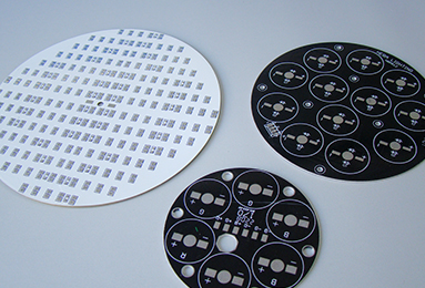
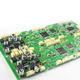
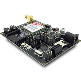
Advanced PCB and Standard PCB
Item Advanced PCB Standard PCB
Application HIGH-END, COMPLEX INEXPENSIVE, FAST
Ideal For Industrial equipments, instrumentation, automotive electronics, communication equipments Children's toys, small appliances, home lighting, functional testing, electronic enthusiasts
Engineering Senior engineer (one file/6 hours) mid-level engineer (5 files/hours)
Production individual working panel mixed working panel
Quantity ≥1 piece 5,10,15,20,25...pieces
Material Lead-free/Halogen-free EM827, 370HR, S1000-2, IT180A, EM825, IT158, S1000 / S1155, R1566W, EM285, TU862HF
High speed Megtron6, Megtron4, Megtron7,TU872SLK, FR408HR,N4000-13 Series,MW4000,MW2000,TU933
High Frequency Ro3003, Ro3006, Ro4350B, Ro4360G2, Ro4835, CLTE, Genclad, RF35, FastRise27
Other Polyimide, Tk, LCP, BT, C-ply, Fradflex, Omega , ZBC2000,
Surface Finishing Spray Tin, Electroless Nickel Gold, Electroless Tin, OSP, Electroless Silver, Gold Finger, Electroless Hard / Soft Gold, Selective OSP, Electroless Nickel Palladium Gold
Ink, Soldermasks Meet IPC4101 class B/L, Rohm&Haas, TAIYO, Kuangshun, Meet IPC-SM-840 class T Meet IPC4101 class B/L, TAIYO, Kuangshun, Meet IPC-SM-840 class T
Plating PTH (Hole copper thickness≥20um), IPC 3(25um) PTH(Hole copper thickness≥18um)
Soldermask Offset ±2mil ±3mil
Dimensional Deviation ±0.13mm ±0.2mm
Warping Angle 0.75% 1%
Test Method A.O.I, Kelvin Four-terminal sensing, Microsection Inspection, Solderability Test, Impedance Test... A.O.I., Fly Probe Testing
Glass Transition ℃ >140℃ >130℃
Package Humidity indicator cards None
Inspection Report Inspection report None
Standard IPC Class 2, IPC Class 3, Automotive Standard, Customer Standard IPC Class 2
Etched Line Forbid to repair tracks(IPC 3, Automotive, Customer Standard) -
Cleanliness Cleanliness requirements beyond those of IPC Meet IPC standards
Certification UL, ISO9001:2008, ISO14001:2004, ISO/TS16949:2009, RoHS etc. UL, ISO9001:2015, RoHS etc.
Layers 120L 2~68L
Maximum plate thickness 14mm(551mil) 10mm(394mil)
Minimum line width spacing internal layer 2.0mil/2.0mil 2.2mil/2.2mil
Outer layer 2.2/2.2mil 2.5/2.5mil
Counterpart Same sheet alignment ±20um ±25um
Interlayer alignment ±4mil ±5mil
Maximum copper thickness 30Oz 6Oz
Hole Diameter Mechanical drilling ≥0.1mm(4mil) ≥0.15mm(6mil)
Laser drilling 0.050mm(2mil) 0.1mm(4mil)
Maximum Size Veneer 1000mmX600mm 850mmX570mm
(Finished size) Backplane 1320mmX600mm 1250mmX570mm
Thickness-to-diameter ratio Veneer 28:01:00 20:01
(Finished Hole Diameter) Backplane 35:01:00 25:01:00
Rapid PCB Prototyping
PCB Order Quantity (m2) Original Lead Time (Days) Current Lead Time (Hours)
0- 50 pcs & < 1m2 2 - 3 Days 24 Hours
1m2 - 5m2 5 - 6 Days 3 - 4 Days
5m2 - 10m2 6 - 7 Days 4 - 5 Days
More than 10m2 8 - 10 Days 5 - 6 Days

Explore Our Works

Sample Title Text
Sample Title Text
Sample Title Text
Sample Title Text
Sample Title Text

FAQ

Here are some Common questions that can help you conduct transactions more effectively.

What does PCB stand for and what services does a PCB board manufacturer offer?

What does PCB stand for and what services does a PCB board manufacturer offer?

PCB stands for Printed Circuit Board. As a PCB board manufacturer, we specialize in designing and producing custom PCBs for various applications, using state-of-the-art technology and materials.

Can I order a custom PCB board tailored to my specific needs?

Can I order a custom PCB board tailored to my specific needs?

Absolutely! We offer custom PCB board services to cater to your unique requirements. Whether you need a specific size, shape, or functionality, our team can design and manufacture a PCB that meets your specifications.

What is involved in the PCB manufacturing process?

What is involved in the PCB manufacturing process?

The PCB manufacturing process includes several key steps: designing the PCB layout, selecting appropriate pcb material, creating the pcb layers, etching the circuit pattern, drilling holes for components, and finally assembling the circuit board components.

How do you ensure the quality of the circuit board components used in your PCBs?

How do you ensure the quality of the circuit board components used in your PCBs?

We source our circuit board components from reputable suppliers and conduct rigorous quality checks. This ensures that all components meet our high standards for reliability and performance.

What are the key considerations in design printed circuit boards?

What are the key considerations in design printed circuit boards?

When we design printed circuit boards, we consider factors like the intended use, required electrical properties, pcb layers, component placement, thermal management, and overall board dimensions to ensure optimal performance and reliability.

What types of PCB material do you use in your manufacturing?

What types of PCB material do you use in your manufacturing?

We use a variety of PCB materials, including standard FR-4, high-speed laminates, flexible materials for flex PCBs, and metal cores for thermal management in applications requiring heat dissipation.

Can you explain the different types of PCB layers and their functions?

Can you explain the different types of PCB layers and their functions?

PCB layers include the substrate, copper layer, solder mask, and silkscreen. The substrate provides structure, the copper layer forms the electrical circuits, the solder mask protects against short circuits, and the silkscreen adds labels for components.

How can I get started with my PCB project?

How can I get started with my PCB project?

To get started, contact us with your project details. Our team will guide you through the process, from initial consultation to final delivery, ensuring your PCB project is successfully realized.

Let's Build Your Product