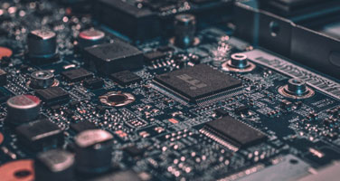
Printed Circuit Boards (PCBs) are the backbone of modern electronic devices, providing a platform for mounting and interconnecting components. Traditionally, PCBs have been manufactured using well-established methods involving photolithography, chemical etching, and multilayer lamination. However, the advent of 3D printing technology is revolutionizing this field, promising to change the way PCBs are designed and produced. This article explores the differences between traditional PCB manufacturing and 3D printing, highlighting their respective advantages, challenges, and future prospects.
1. Photolithography and Etching:
Traditional PCB manufacturing starts with a substrate, usually made of fiberglass (FR4) or similar materials, coated with a layer of copper. The desired circuit pattern is transferred onto the copper using a photosensitive film. This is exposed to ultraviolet light through a mask, hardening the exposed areas. The unexposed areas are then washed away, leaving a pattern of copper that forms the circuit. This process is known as photolithography.
Next, the board undergoes chemical etching, where an acid bath removes the unprotected copper, leaving behind the circuit traces. After etching, the board is cleaned, and additional layers can be added using similar methods to create multi-layered PCBs.
2. Drilling and Plating:
Holes are drilled into the board to allow components to be mounted and interconnected. These holes are then plated with copper to ensure electrical conductivity between layers. Drilling and plating are precise operations, crucial for ensuring the functionality and reliability of the PCB.
3. Solder Mask and Silkscreen:
A solder mask is applied to insulate the copper traces and prevent short circuits. This is typically a green (though other colors can be used) epoxy resin that is hardened through heat or UV light. Finally, a silkscreen layer is added to print labels and component markings on the PCB, aiding in assembly and maintenance.

1. Established Process:
Traditional PCB manufacturing is a well-established, mature process with decades of refinement. This ensures high reliability and consistency in the final product.
2. High Precision:
Photolithography and etching provide high precision, capable of producing fine traces and intricate designs necessary for modern electronics.
3. Cost-Effectiveness at Scale:
For large production runs, traditional methods are highly cost-effective. The initial setup costs (masks, etching baths, etc.) are offset by the economies of scale in mass production.
4. Material Versatility:
Traditional methods support a wide range of materials and substrate types, allowing for customization based on the specific requirements of the application.
1. Initial Setup Costs:
The initial setup involves significant costs, including the creation of masks and the procurement of chemicals and equipment. This makes small production runs less economical.
2. Time-Consuming:
The multiple steps involved in traditional PCB manufacturing are time-consuming, especially for complex multi-layer boards.
3. Environmental Impact:
The chemicals used in etching and plating are hazardous and require proper disposal and recycling, adding to the environmental footprint of the process.
3D printing, or additive manufacturing, is a process where material is deposited layer by layer to create a three-dimensional object. When applied to PCB manufacturing, 3D printing offers several transformative advantages.
1. Direct Digital Manufacturing:
3D printing allows for the direct digital manufacturing of PCBs from CAD files, eliminating the need for masks and etching baths. The design is directly translated into a physical object using conductive and insulating materials.
2. Multi-Material Printing:
Advanced 3D printers can print with multiple materials simultaneously. This capability enables the creation of conductive traces, insulating layers, and even the embedding of components in a single print cycle.
3. Rapid Prototyping:
One of the most significant advantages of 3D printing is the ability to rapidly prototype and iterate designs. Changes can be made digitally and printed within hours, significantly speeding up the development cycle.
4. Customization and Complexity:
3D printing excels in producing complex and customized designs without additional costs. It allows for the creation of unconventional geometries and integrated structures that are difficult or impossible to achieve with traditional methods.

1. Reduced Lead Times:
By eliminating the need for masks, chemical baths, and multiple processing steps, 3D printing drastically reduces lead times from design to final product.
2. Cost-Effective for Small Runs:
3D printing is highly cost-effective for small production runs and prototypes, as it does not involve high initial setup costs.
3. Environmental Benefits:
3D printing generates less waste and uses fewer hazardous chemicals compared to traditional methods, making it a more environmentally friendly option.
4. Enhanced Design Flexibility:
Designers can experiment with new layouts and materials without the constraints imposed by traditional manufacturing methods, fostering innovation.
1. Material Limitations:
While 3D printing materials are continually improving, they still lag behind traditional materials in terms of electrical conductivity and thermal properties.
2. Resolution and Precision:
The resolution and precision of 3D printers are currently not as high as those achieved through photolithography, limiting their use for extremely fine-pitch components.
3. Equipment Costs:
High-end 3D printers capable of producing functional PCBs are expensive, which can be a barrier for small businesses and hobbyists.
4. Limited Multi-Layer Capabilities:
Although multi-material 3D printers are available, the complexity of creating reliable multi-layer PCBs with embedded components is still a challenge.
The future of PCB manufacturing is likely to see a convergence of traditional methods and 3D printing. Hybrid approaches that leverage the strengths of both techniques are already emerging. For example, 3D printing can be used for rapid prototyping and initial design iterations, while traditional methods can be employed for high-volume production runs.
1. Improved Materials:
Ongoing research into new materials for 3D printing promises to close the gap in conductivity and thermal performance, making 3D printed PCBs more viable for a broader range of applications.
2. Enhanced Printing Technologies:
Advancements in 3D printing technology, including higher resolution and faster print speeds, will continue to improve the precision and feasibility of 3D printed PCBs.
3. Integrated Manufacturing:
Future manufacturing processes may integrate 3D printing with traditional methods, such as combining 3D printed substrates with traditional copper plating and etching techniques to optimize both cost and performance.
4. Customization and On-Demand Production:
As 3D printing technology becomes more accessible, it will enable greater customization and on-demand production of PCBs, catering to niche markets and specialized applications.
Market Data and Trends
| Market Size and Growth | According to a report by Market Research Future, the global PCB market was valued at approximately $60 billion in 2021 and is projected to reach $75 billion by 2026, growing at a CAGR of around 5%. The adoption of 3D printing in PCB manufacturing is a key factor driving this growth, as it allows for faster production cycles and customization. |
| Adoption Rates | A survey conducted by IDTechEx revealed that about 20% of PCB manufacturers have already integrated 3D printing technologies into their processes, primarily for prototyping and low-volume production. This number is expected to rise to 50% by 2030 as the technology matures. |
| Cost Comparison | For traditional PCB manufacturing, the cost per square inch for high-volume production can be as low as $0.05, while for 3D printed PCBs, it currently ranges from $0.50 to $2.00 per square inch, depending on the complexity and materials used. However, the cost gap is expected to narrow as 3D printing technology advances and becomes more widespread. |
| Lead Time Comparison | Traditional PCB manufacturing typically requires 2-4 weeks for design, prototyping, and production, while 3D printing can reduce this to a few days. This reduction in lead time is particularly advantageous for industries that require rapid iteration and quick time-to-market. |
| Environmental Impact | 3D printing can reduce material waste by up to 90% compared to traditional PCB manufacturing, according to a study by the Fraunhofer Institute. This significant reduction in waste, combined with fewer hazardous chemicals, makes 3D printing a more sustainable option. |
In actual circuit board design, functional partitioning needs to be carried out according to specific application scenarios and requirements. For example, in high-performance computer motherboards, key modules such as CPU, memory, and graphics cards may need to be partitioned separately to improve performance and stability; in miniaturized smart devices, factors such as space utilization and heat dissipation design need to be fully considered. You should also choose a matching method based on specific needs.

Leading provider of advanced PCB Assembly (PCBA) solutions. Our state-of-the-art manufacturing facility has an impressive infrastructure with a total of 9 Surface Mount Technology (SMT) production lines and 4 dedicated Dual Inline Package (DIP) assembly lines.
At Huaxing PCBA Factory, we pride ourselves on our commitment to providing PCBA solutions that consistently meet and exceed the highest industry standards. Our strong Quality Management System (QMS) is the cornerstone of our operations, ensuring that every product leaving our facility is of the highest quality.
If you have needs, you can contact us to help you.

